

Description
Here I describe how I came up with the idea of replacing conventional FR4 circuit boards with 3D printed versions that also can integrate components, structure and cosmetic surface of the product. In the end I provide some tips for creating 3DPCBs. More posts will follow where I use this technology in different products and this post describes how to make a refined version of the 3DPCBoy gaming device, featured above.
Features
- Rapid manufacturing, no need to wait for PCB production and shipping.
- No special equipment or materials needed (just an FDM 3D printer, soldering station and wires.
- Integrated wire guides show how connections are routed (beginner friendly).
- Allows 3 dimensional circuits, opening up for new ways of integrating electronics, reducing size, part count and complexity.
- Low cost
First of all, I would like to state that I’m sure that similar ideas have been developed before. I don’t claim that this is revolutionary and it certainly comes with pros and cons. The concept shares parts of perfboard designs, various 3D printed designs, wire warp and dead bug soldering. The combination of these techniques, its simplicity and possibility to integrate electronics and casing is quite promising, and by sharing this idea I hope that the method can evolve and be combined with new inventions to become even better.
Development – Day 1
I recently got a spare weekend (which is quite uncommon these days) and decided to use the time to play with different ways of making a PCB with a 3D printer. I wanted to see to what extent one can use standard technology, so I skipped printed metal, conductive filament and silver epoxy and similar solutions. Preferably I would rely on a single head FDM printer with PLA filament and reliable connections (solder or maybe even wire wrap). The plan was to test different ideas, iterate small steps and see what comes out. It’s a nerdy way to spend a weekend, but I really like the creative process of making something new.
My first idea was to use through hole components and bend the wires so they act like traces on a PCB. This is normally called fly-wire, point to point or sometimes dead bug circuits. However, the difference would be to use a 3D printed structure as support, simplifying the soldering process, guiding the user and making the final solution sturdier.
I needed to start somewhere, so I created a miniature Arduino breakout board (since they are simple and always handy). The process was similar to an ordinary PCB, with the only exception that the traces were replaced by the component legs.

When I was satisfied with the 2D sketch, I created a 3D model of the support board and printed it using standard PLA.

The printed board was then used to test if the concept was working. The biggest risk was that the PLA would melt when soldering the wires, but luckily the soldering process is quite fast and even if the PLA get soft, it cools quickly and keeps its shape. For absolute beginners this might create a problem if you apply too much heat, but once you have soldered a few connections this should work fine.

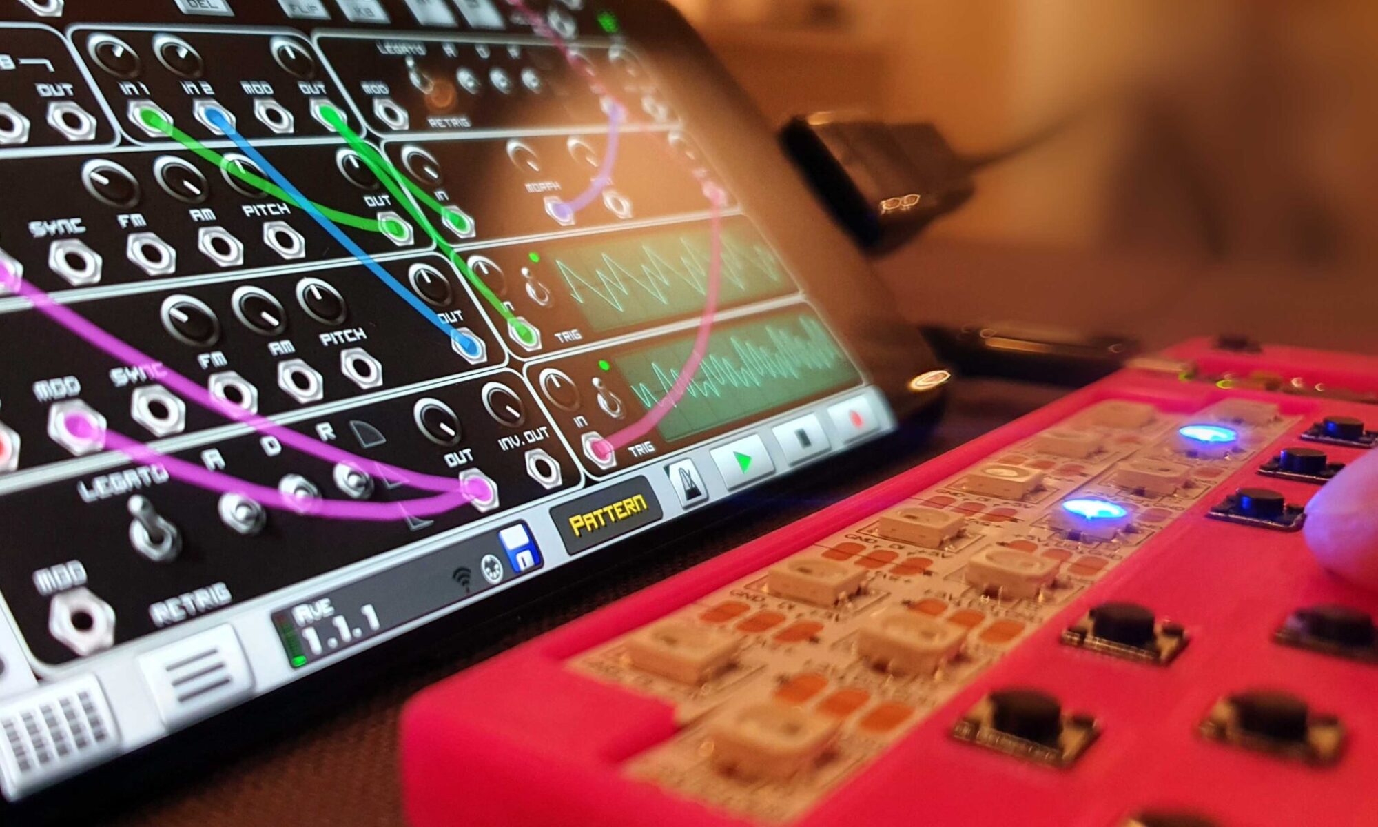
The concept showed potential, but I realized that I needed to guide how the wires should be connected. If only there was a way of integrating guide channels to the model… This was easily solved by adding an extra layer on the circuit board that had channels for the connections. I even added a frame, allowing the circuit to lay stable on a flat surface and reducing the risk of short circuit the wires.

3D printing the board took 40 minutes with a BNC3D with 0.4mm nozzle and 0.15mm layer height using standard settings in Cura (without support & 205 deg C for the colored PLA).
Once the board was printed, soldering was straight forward, starting with the atmega328 and the low height components, bending the wires, soldering the connections and cutting away anything that protruded the frame. Since the component legs have limited length, I had to add two pieces of wire (0,5mm tinned copper wire). It’s actually fewer solder joints than a PCB, since two connections (component – PCB – component) are replaced by one.

The breakout board is obviously not Arduino shield compatible and you need to add a bootloader before programming it using a USB to serial adapter (this can be done using another Arduino – google it if you don’t know how).
After several iterations I had now reached the end of the first day and I felt that the concept had great potential. Just imagine when you don’t want to wait for a PCB order or the endless possibilities to add 3-dimensional shapes to the board. It doesn’t need to be flat anymore and it’s easy to integrate keycaps, attachment brackets or battery holders into the PCB itself…
Day 2 – game time!
After a good night’s sleep, I was eager to continue to experiment with the concept. Since the Arduino breakout board worked, I decided to build something with more complexity. An Arduboy clone seemed like the perfect next step. It has an OLED display, some pushbuttons, a beeper and most importantly you can play games on it! It would be awesome if you could print the PGB and solder a working handheld game without the need for perfboard or a custom-made PCB.
I started designing in 2D by creating models for the different components and positioned them in order to build a compact device. By placing the Arduino pro micro beneath the OLED display I could keep a small form factor. Compared to the original Arduboy I did some modifications:
- Only PIN5 connected to the beeper (the other side to GND)
- I removed the RGB LED (might be added in the future)
- CS pin of the OLED connected to GND (since the SPI is not shared)
I then routed the connections with an iterative approach. After testing a couple of different tracks, I had a solution with good spacing between the traces and only a single bridge (where wires cross each other and needs to be separated to avoid short circuit).

From the 2D routed drawing I created a 3D model similar to the Arduino breakout board. One layer with holes for the components, one layer with cut-outs for the traces and one layer for the frame. Everything was printed upside down. After one-hour printing time I could assemble the first version.


To keep the shape of the traces I used a rather sturdy 0.5mm tinned copper wire. It was not a problem assembling the device, but I realized that the 2mm wide cut-out was too spacious, and the rather thick wire was a bit tricky to bend correctly. Since I wanted something that could be assembled quick and easy, I realized that I had to optimize the wire and channels and probably needed to test lots of different options. To save time I created a compact board (2x2cm) with three test traces. I then tested altering the sizes of the channels and could quickly test different wire diameters. I noticed that a thinner wire was easier to route, but needed better guiding since the wire is less stiff compared to the thicker. I realized that I could use the 3-dimensional freedom and created traces that was bigger inside the board with just a narrow opening on the top. In the cross section, the channel had a diamond, or rhombus shape, where only the top protruded the board. The diamond shape has several advantages compared to a circle, it is easier to print the constant angle undercut and the .STL file becomes much lighter. With this approach it was easy to insert the wire and by stretching it slightly it was kept in position. I tested different openings and different sizes of channels before I found the optimal setup.


The channels were created by placing the a diamond / rhombus curve at the end of the routed trace continued by a solid rail extrusion. The extrusions were then subtracted from the main board.
I also tested different wire options and found that the best result was using a 0.3mm diameter copper wire (0.07mm2 area) that I got from strands of RK-wire (the multi strained cable used for internal wiring in electrical 230V cabinets). It is easy to route yet still keeps its shape.
I like to kill my darlings, so I also tested a version where I used the soldering iron to melt the wire in dedicated pins along the trace. This method worked, but it was quite time-consuming and the melted plastic is probably not good for the health, nor the soldering iron. A more successful method was to create smaller straight channels that alternated between the two sides of the board. With this setup, I basically sewed the wire in position. It worked great, but was more time-consuming compared to the diamond trace.
I was worried that the diamond method was sensitive for printer calibration and tested if it worked printing upside down (with the trace opening against the glass of the 3D printer). It worked just as great as printing it with the opening on the top side.
With the new approach I remodeled the Arduboy 3DPCB and printed a second version. When I used the thinner wire, I noticed that the assembly process improved a lot.


However, it also became apparent that using the traditional 45 deg routing method was not optimal for wire bending. I decided to take a shot at this too, and made a copy of the model and rerouted all the tracks, this time trying to keep each trace as straight and short as possible. This is called topological routing and creates a board that doesn’t look like an ordinary PCB, but I guess that this is not an ordinary PCB, so looks aside, this is a better approach where the sharp angles are replaced by circle segments. (note to self – try curvature-contingent routing one rainy day…).
Just by curiosity, I measured the length of the traditional 45 deg routing (509mm) with the topological routing (463mm) – it’s not a big difference, but still.

Since the wires are embedded in the structure, I could now remove the frame. This allowed me to print with component side up and I could integrate support structure and protective cover on top of the board. This is where the advantages of the technology really become apparent, and the board and case become one. I added support pins for the OLED display and extruded a tube inside the block to create a hidden wire crossing. It’s almost overkill, but demonstrates that you can do lots of new things that are not possible with traditional stack ups. To improve assembly, I added extra cut-out where the soldering should be done, it’s now easy to see not only how the wires should be placed, but also where to solder the board.


When the integrated board was printed and tested it was early Monday morning. I haven’t had this much fun in a long time, I missed some meals, hardly slept, but did lots of experimenting and testing new ideas, several bad ones, but a few good ones make it all worth the effort. I hope that this method will be used by others and I can’t wait to develop more projects with 3DPCBs to see how far the idea can be developed. It would be fun to create a synth or maybe a printed computer with blinkenlights…
Pros:
- No need to wait for PCB delivery
- Can be made with a standard 3D printer
- Low cost (filament and some copper wire)
- Large number of color options
- Shape not limited to flat sheets, can easily integrate support, battery connectors and outer case.
- Fewer solder joints when you use the component legs as wires.
Cons:
- Large pitch compared to what can be done with SMD PCBs – mainly suitable for through hole components.
- Soldering takes slightly more time compared to a regular PCB since you need to add the wires (but it’s a quite fast process anyway).
- Heat sensitive compared to FR4. It’s not fire retardant and will melt if heated – NEVER EVER USE 3DPCBs for high voltage or large currents!
- No available tools for routing, it has to be done manually in 3D CAD.

Tips for designing a 3DPCB
After the initial weekend I have iterated the design of the 3DPCBoy and created other projects. Over time I have learned a few tricks that makes designing 3DPCBs easier:
- Avoid hidden bridges – Its cool that they are feasible, but even with a fixed radius (subtracting a torus), there is a risk that the print isn’t perfect and threading the wire can be difficult. Use both sides of the board and simply switch side with one hole, cross the wires and go back with another hole.
- Use a modular design in the CAD software, separate routing, 3D extruded tracks, board and 3D objects. Use Boolean subtraction to create the wire paths and save the extrusions if you want to edit something later.
- Try to design without the need for 3D printed support structures. Add chamfered cut-outs where you need to solder, like connecting a wire to a switch.
- Bending component legs; locks them in position, reduces height, avoids short circuit and is easier to solder.
- I have now tried curvature contingent B-spline routing and it works great. It automatically avoids straight lines which keeps the wires in place. The downside is that it’s a bit more time consuming to route, and it also looks funny compared to normal routing. If you expect that the model will be used by many curvature routing is recommended. If it’s a one off, straight lines and radiuses works well.

Bill of Materials (BOM)
- FDM 3D printer with PLA filament
- Solder station & solder tin
- Thin wires. I used 0.3mm copper wires (strands from 20cm of RK-wire)
- Components for whatever you are building, see separate post for the 3DPCBoy.
Licensing

This work is licensed under a Creative Commons Attribution-NonCommercial-ShareAlike 4.0 International License.
Really interesting concept. Have you tried other designs. Kudos
Sure. I have posted a watch that uses the same idea https://vonkonow.com/wordpress/2020/01/colourful-connected-clock/, and I will release a few more that shows the possibilities with 3DPCB.
/j
Awesome work dude!
Do you think it’s possible to modularise this like a DIY littlebits? That would be extremely user friendly and very cheap compared to the price of the littlebits product.
That’s an interesting idea. The magnetic connectors might be tricky to build, but definitely not impossible. I also like how grove modules are connected in a modular way with i2c and power.
https://www.seeedstudio.com/Grove-Beginner-Kit-for-Arduino-p-4549.html
Most of the modules could definitely be rebuilt with 3DPCB…
there is a fly tying thread wrapping tool- holds a spool of thread and has a very thin tube that guides the thread in tiny spaces.
Use a spool of thin copper wire, and you could install wires into the slots very quickly and easily, and even wrap them a turn or two around the component lugs to make soldering easier.
There is even very fine magnet wire that has insulation that melts at soldering temps….
Oh Darn! You invented the 3DPCB already :(
Nevermind – I came up with a similar solution using deep groves and double-sided component mounting.
I’ll be making a video soon as there are differences.
Making a 3DPCB is really the way to go for small, compact prototyping whilst eliminating stuff like the connectors.
Well done – great article and you do amazing projects!