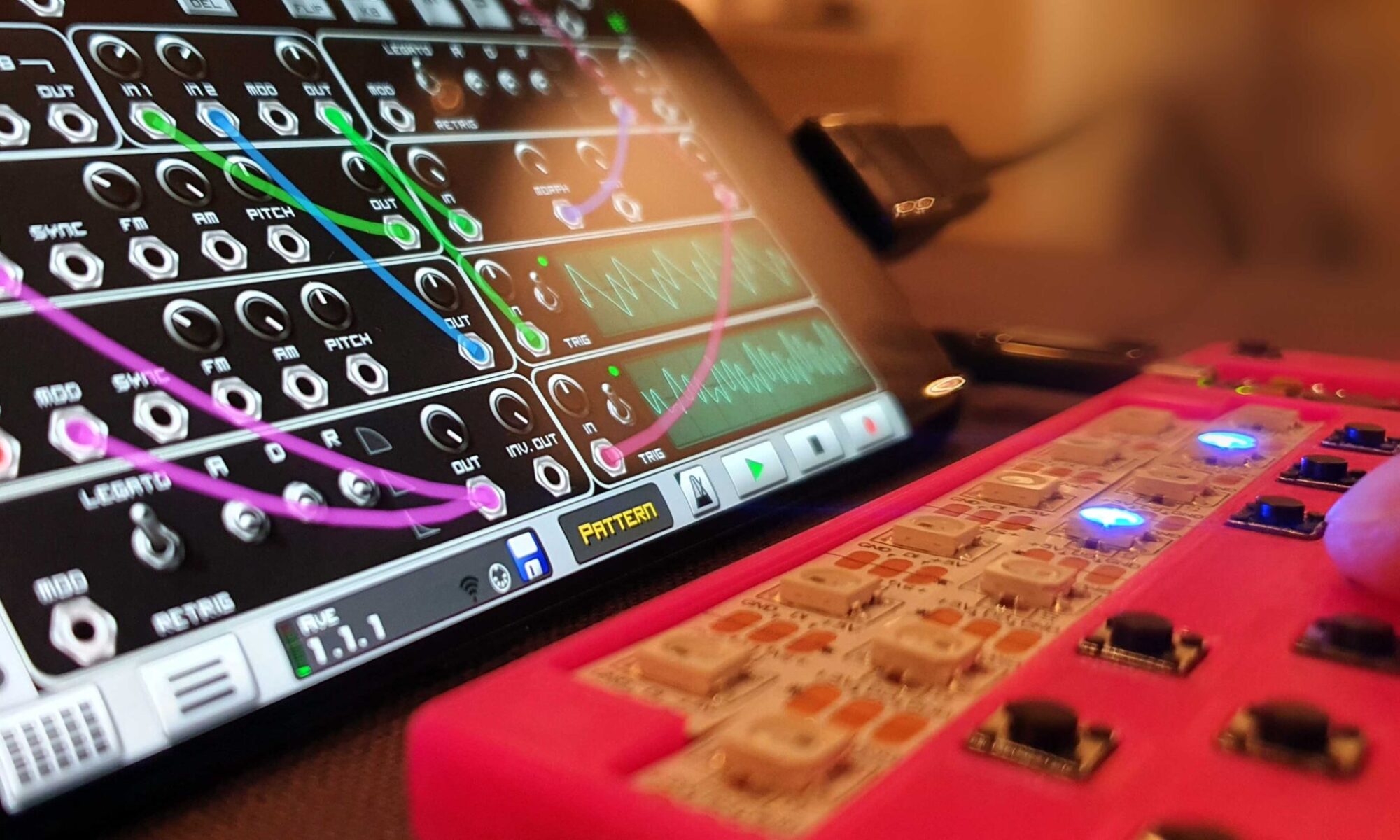
The Pad MIDI keyboard is part of the LEET Synthesizer project. If you haven’t – It is a good idea to read the main post first before continuing with the details below:
This post describes how the pad keyboard works and what you need to build your own.
Description of the Pad

Part list:
Component cost is around $6 on eBay October 2020 (will depend on shipping and supplier).
- 1x 3D printed core 3DPCB
- 1x Arduino pro micro, or compatible clone (5V version. ATmega32U4) – (~$4)
- 11x 6x6mm 4pin through hole tact switches – preferably with low activation force (50g / 0.5N) – ($0.2)
- WS2812 LED-strip with 8 LEDs (60 LEDs/m. I used IP60, white FPC) – ($1.1)
- 1x 25cm RK wire (containing 24 strands of 0.3mm copper wires) – ($0.1)
Equipment:
- 3D printer (FFF/FDM with PLA filament)
- Solder station with a narrow tip
- Basic tools: needle- and cutting pliers, knife, hot-glue
- Computer to run Arduino IDE and upload firmware (using a Micro USB cable)
Build it
I have not made a step by step building instruction, but check out the video and illustration below. The build process is very similar to the step by step instruction for the keyboard.

Development
The pad is literally a smaller version of the LEET keyboard. I rearranged the LEDs and switches, downsized it, rebuilt the 3D model and adjusted the code.
Download project files

All files required for this project are available at this GitHub repository:
https://github.com/vonkonow/LEET-Synthesizer/tree/main/Pad
License

This project is open source under MIT License
(Attribution is optional, but appreciated /Johan von Konow ;)


Hi Johan. Big project!
But I think at
https://github.com/vonkonow/LEET-Synthesizer/tree/main/Pad
you has been confused and included the code from LEET-CONTROL.INO instead of LEET-PAD.INO
I will be very grateful if you share the correct code.
Thanks!
Hi Andrés
Thank you for finding this error. It is now corrected (the right code is in the repository).
Sorry for any trouble.
/j
There is something that should be (IMHO!) more explicit here, even though yes, I’ve built the keyboard and it IS consistent with that — but it should be EXPLICIT (good engineering! :-) — and it is actually slightly different, which is where I had confusion.
(Here’s why: the keyboard lower light strip had 2 wires on one side and 3 on the other; this has 2 wires on each side of both light strips, and now a wire in the middle of the strip? — so which orientation should each light strip be?)
I was able to figure out from both a little logic – but even better: the PAGE-graphic at the top of this page shows the LEDs’ “maze” orientations, as well as +/-/-> signs that makes it easy to figure out, IF you trust it. (A webpage header graphic is NOT “engineering instructions” – but in this case it was the best I had, and it agreed with what I then figured out was the electrical pathway…. :-)
The bottom strip: DO on left, DI on right, so obviously you solder wires to the bottom two pads (bottom-most is GND on either end) (and ignore +5v on both ends!).
The top strip: DI on left, DO on right. Solder wires to the bottom two pads – now the 2 bottom pads are the +5v, which is good, because otherwise we wouldn’t have any power! :-). And solder wires where the holes in the middle of the pad go — at this point it’s where the wire fits. But as you can see compared to where the other wire holes are at each end – you’re connecting +5v to +5v, so the top pad of the bottom strip goes to the bottom pad of the top strip – between the 1st and 2nd LEDs.Common power.